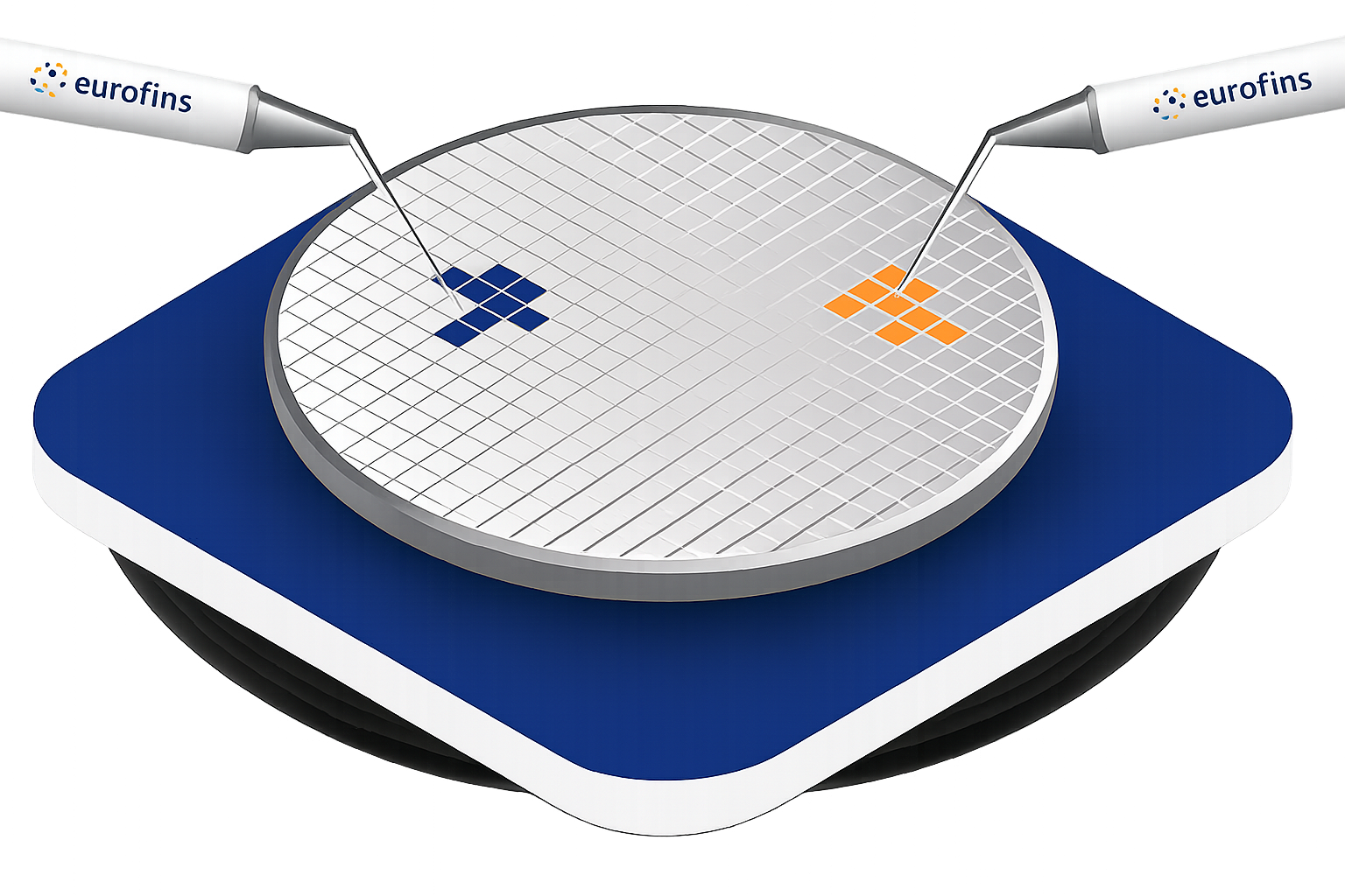
Aptasic offers multi-site wafer probing starting from 4” wafers up-to 12” wafers. Tests can be performed at COLD, AMBIENT and HOT ranging from -40°C to 125-200°C.
Multi-site
We develop Hardware and Test Software concepts to optimize the multi-site test up to 16 parallel site probing.
The idea is to make the most efficient use of the test system resources to cover the requirements.
Aptasic has developed a flexible concept for dedicated hardware implementation.
This concept includes cantilever or vertical probing technologies, Specific DUT boards and standards / custom load-boards.
CMOS Imager
Aptasic has a complete test concept in place for CMOS Imagers on 12 inches wafers. The Test SW structure is structural and functional to secure the qualitative and the quantitative aspects of the imager.
Light stimulation concept is also applicable for various wavelengths and the environment is fully updated to comply with very high sensitivity devices.
This particular competence and appropriate equipment set up has been proven over the last years and we can provide a high level of quality using cost effective methods.